GLAS-PPE/97-0427 August 1997
Semi-insulating, undoped, Liquid Encapsulated Czochralski (SI-U LEC) GaAs detectors have been irradiated with 1MeV neutrons, 24GeV/c protons, and 300MeV/c pions. The maximum fluences used were 6, 3, and 1.8 1014 particles/cm2 respectively. For all three types of irradiation the charge collection efficiencies (cce) of the detector are reduced due to the reduction in the electron and hole mean free paths. Pion and proton irradiations produce a greater reduction in cce than neutron irradiation, with the pions having the greatest effect. The effect of annealing the detectors at room temperature, at 200oC and at 450oC with a flash lamp have been shown to reduce the leakage current and increase the cce of the irradiated detectors. The flash-lamp anneal produced the greatest increase in the cce from 26% to 70% by increasing the mean free path of the electrons. Two indium-doped samples were irradiated with 24GeV/c protons and demonstrated no improvement over SI U GaAs with respect to post-irradiation cce.
The possible use of GaAs detectors in the future ATLAS experiment at the LHC imposes severe demands on the radiation hardness of the GaAs detectors. Semi-insulating, undoped GaAs detectors have been shown to withstand doses up to 100Mrad of 60Co gamma rays [1]. Their sensitivity to neutrons, protons and pions are reported in this paper.
The irradiations were performed at the ISIS facility [2] for the neutron exposure, with a spectrum strongly peaked at 1MeV, the CERN PS for 24GeV/c protons [3] and the PSI, Villigen, for 300MeV/c pions [4]. All irradiations were performed at room temperature.
All the detectors (except for two described in section 6) were fabricated with SI U GaAs substrates [5], with thicknesses varying from 115mm to 500mm. The substrates were lapped and polished at Glasgow University to obtain the desired thickness. Various thicknesses were used so that the dependence of the leakage current and charge collection efficiency on this parameter could be studied. All the detectors had 3mm diameter circular pad contacts with a 200mm wide guard ring separated from the pad by 10mm. The Schottky contact on one face of the wafer was metallized with Ti/Pd/Au and the ohmic contact on the other face was Pd/Ge annealed at 300oC. The leakage current characteristics before and after the irradiations were obtained with a Keithley 237 voltage source measurement unit. A 90Sr source was used to determine the response of the detectors to minimum ionising particles with an amplifier shaping time of 500ns. The charge collection efficiencies of either electrons or holes created in the first 20mm of the detector thickness were obtained with the use of an 241Am alpha particle source placed on the Schottky or ohmic contact, respectively. An amplifier with a 500ns shaping time was used. The current characteristics and charge collection efficiencies from the 90Sr source were obtained at both 20oC and -10oC. The -10oC temperature was chosen as this is the proposed operating temperature of the ATLAS semiconductor tracker.
The effect of all three types of irradiation on the reverse current characteristics of the GaAs detectors is small.
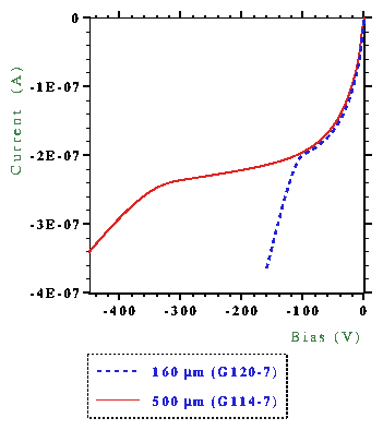
Reverse current characteristics of two detectors of different thickness, 160mm and 500mm, both of which were irradiated to 6 × 10¹³ p/cm2 are shown in figure 3. It can be seen that the value of the leakage current up to Vfd is independent of the detector thickness. This is not the case in silicon where the leakage current, Ir, has a dependence on fluence, F, given by [6]
| (1) |
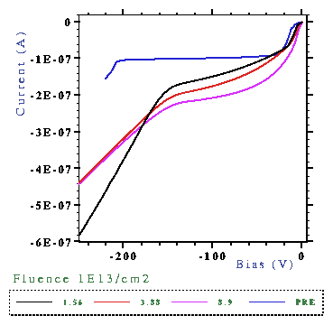
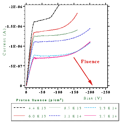
The forward current characteristics also change with increasing fluence. The effect of protons on a 160mm thick detector, shown in figure 4, illustrates this. A plateau appears that extends to higher bias values with increasing fluence while the magnitude of the plateau current falls. This allows the detector to be operated under forward bias.
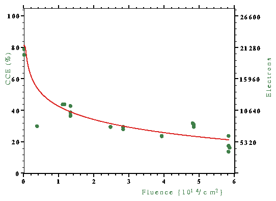
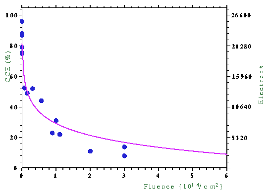
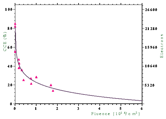
The charge collection efficiencies for 200mm thick detectors as a function of neutron, proton and pion fluence are shown in figures 5, 6 and 7. These were measured using minimum ionising particles (mips) from a 90Sr source at an applied bias of 200V. The reduction in cce with fluence occurs at a greater rate for pions and protons than for neutrons. A 10000 electron signal response to the 90Sr source, ( � 40% cce), is obtained after 1.4 × 10¹⁴ n/cm2, 6.0 × 10¹³ p/cm2, and only 3.0 × 10¹³ p/cm2. The cce falls rapidly initially and then at a slower rate for higher fluences with the position of the change in gradient depending upon the particle type.
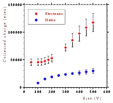
Irradiated 200mm thick detectors biased in excess of 200V demonstrate an increase in cce. For example for a 160mm thick detector irradiated to a fluence of 1.0 × 10¹⁴ p/cm2 the signal increased from 8500 electrons at 200V to 12000 electrons at 400V. The reason for the increase in signal can be understood from the electron and hole collection data. Before irradiation, the signal due to the holes is greater than that due to the electrons, implying that the electrons are trapped more than the holes. The signal due to the holes however falls at a faster rate with fluence than that due to the electrons. This means that both electron and hole traps are introduced with irradiation, while the electron trapping is the less important after irradiation contrary to what is observed in unirradiated detectors. The electron signal, which is constant for a bias up to Vfd, rises at greater applied biases as shown in figure 8. The hole signal remains almost constant with increasing bias after its initial steep rise at Vfd. From this it is possible to conclude that field-enhanced electron detrapping may be present.
As the mip signal for a GaAs detector irradiated in excess of 1.0 × 10¹⁴ p/cm2 appears to be independent of substrate thickness, even at an applied bias much larger than Vfd, it is proposed that the carriers have a mean free path less than or equal to the thickness of the thinnest detector tested, that is 115mm. The charge deposited by a mip, Qdep is given by
| (2) |
| (3) |
| (4) |
| (5) |
| (6) |
The change in the reverse current of a detector irradiated to 1.0 × 10¹⁴ p/cm2 has been measured over a period of time greater than 1 year. The sample was stored at room temperature, which varied throughout the year from 18oC to 25oC. All the current measurements were carried out at 20oC with the same Keithley 237 voltage source measurement unit. The first current measurement was performed 20 days after the irradiation period due to the initial activity of the sample and holder preventing earlier handling. The value of the reverse current, Ir, at Vfd reduced with time (t), in hours, with a logarithmic dependence given by
| (7) |
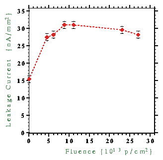
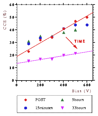
Elevated temperature annealing, for periods ranging from 15 minutes to 33 hours, was performed on six irradiated detectors in an oven at 210oC in air without bias. The reverse current and charge collection efficiency variations for a 180mm thick detector irradiated to 1.0 × 10¹⁴ p/cm2 are shown in figures 9 and 10. The reverse current decreased after an 33 hour anneal from 0.22mA to 0.14mA (corresponding to 30nA/mm2 to 20nA/mm2) where the unirradiated value was 0.10mA (14nA/mm2). The full depletion voltage remained unaffected by the annealing. For an applied bias of 100V the cce increased from 23% to 30% for annealing times up to 5 hours. As the bias increased, the increase in cce for the annealed detector was at a slower rate than in the pre-annealed case, resulting in a lower cce for the annealed detectors at biases in excess of 400V. For longer anneal times the cce decreased. For an anneal time of 33 hours, for example, the cce was only 15% at 100V rising to 22% for a maximum applied bias of 500V.
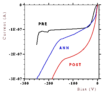
The arsenic antisite defect in GaAs is known to anneal at temperatures in excess of 450oC [8]. As the irradiation could produce such antisite defects the effect of annealing at 450oC was investigated. A flash-lamp anneal was used to illuminate the detectors for either 30,60,90, or 120 seconds. The effect was shown to be independent of the detector side which was illuminated, demonstrating that the whole bulk was being heated. The plateau reverse leakage current was reduced but so was the full depletion voltage. For an applied bias greater than Vfd the annealed current was greater than before annealing with the gradient of this section of the current characteristic being quite large. The mip cce of the detector was increased for applied biases less than Vfd, however due to the large increase in leakage current above Vfd it was not always possible to measure the charge collection at a higher applied bias. The increase in mip cce was due to an increase in electron mean free path with anneal time while the hole mean free path remained unchanged. A bias of 300V, which could be applied to a detector annealed at 450oC for 120s after a fluence of 1.7 × 10¹⁴ p/cm2, gave a mip cce of 71%. The pre-irradiation cce was 95% and the post-irradiation, pre-anneal value was 26%.
Two detectors were fabricated with 500mm thick SI GaAs doped with indium [5]. These were tested before and after an exposure of 1.4 × 10¹⁴ 24GeV/c protons/cm2. The reverse current of the detectors before irradiation was 30nA/mm2, less than for the 500mm thick SI-U GaAs detectors. After the irradiation the value of Vfd was reduced to only 220V, compared to 340V for the undoped sample. The current at the applied bias of Vfd was 0.4mA (57nA/mm2) which was higher than that of the undoped sample which was 0.22mA. The charge collection efficiency for the indium doped samples was less that that of the undoped samples before irradiation by 20%. After the irradiation the signal fell to 10% (6650 electrons) compared to 17% (11305 electrons), respectively, for an applied bias of 1000V.
The changes in reverse current and charge collection efficiency for SI-U GaAs detectors have been studied after irradiations with 1MeV neutrons, 24GeV/c protons and 300MeV/c pions. While the leakage current variations are slight and pose little problem to the operation of the detectors, the fall in cce gives major cause for concern. At a given high fluence, the reduction is greater for charged hadrons than for neutrons (this difference is discussed in detail in reference [9]). The cce falls rapidly in the first 3 × 10¹³ p(p)/cm2. The reduction has been shown to be due to both electrons and holes being trapped, with the hole mean free path affected much more dramatically. For an applied bias greater than Vfd the cce increases due to the increased signal from the electrons. Room temperature annealing has been identified in the reverse current characteristics and a slight improvement has also been seen in the cce. Annealing at elevated temperatures has shown beneficial effects in both leakage current and cce. The effect of proton irradiation on indium-doped GaAs detectors has shown the material to be no more radiation-hard than SI-U GaAs. Further tests on different samples should be performed.
The authors would like to thank F.McDevitt, A.Meikle and F.Doherty for technical support and all those at the ISIS, CERN PS and PSI facilities during the irradiation runs. One of us (R.Bates) gratefully acknowledges the support received through a CASE postgraduate studentship from RAL. The results obtained within the RD8 collaboration are from work partly funded by PPARC (UK), INFN (Italy), and the BMFD (Germany).