


Next: RICH Prototype
Up: HPD development
Previous: Pixel HPD
The pad HPD will be housed in a cylindrical glass envelope capped with
a UV-glass entrance window with a
K2CsSb photocathode.
A visible light photocathode deposition facility that allows a
high vacuum
seal of the HPD baseplate onto the metal flange of the glass envelope
has been designed. The final
assembly of this apparatus was performed at CERN at the end
of 1997. The signal from the photoelectrons in the silicon sensor will be
detected by front end chips
placed around the edge of the sensor via wires
bonded to the routing lines from the pad. Focussing electrodes, fixed
in the glass envelope, will demagnify the image by a factor of 2.3. The
2048 pad silicon detector contains pads of dimensions
1 1mm2. Successful tests have been performed on the sensor with
photoelectrons up to 20 keV with (the non LHC speed) VA3 chip [7].
A signal/noise ratio of
1mm2. Successful tests have been performed on the sensor with
photoelectrons up to 20 keV with (the non LHC speed) VA3 chip [7].
A signal/noise ratio of
 10 has been achieved. Earlier tests
with a 256 pad sensor had achieved a signal/noise ratio of
18.
This difference is under investigation, but one possible reason for this
degradation in performance is differences in the manufacturing of the
wafer.
10 has been achieved. Earlier tests
with a 256 pad sensor had achieved a signal/noise ratio of
18.
This difference is under investigation, but one possible reason for this
degradation in performance is differences in the manufacturing of the
wafer.
The SCT-128A [8] analogue chip which was developed for the
ATLAS silicon tracker is being modified to achieve a noise level of
 600e-. Additional modifications will be needed to meet the
requirements of the pad HPD for LHC-B, in particular the multiplexing
properties of the chip.
600e-. Additional modifications will be needed to meet the
requirements of the pad HPD for LHC-B, in particular the multiplexing
properties of the chip.
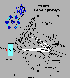
Figure 3:
Configuration 1: the 1/4 scale prototype RICH vessel
 |
Next: RICH Prototype
Up: HPD development
Previous: Pixel HPD
Converted by www person
1998-02-26