In simulating a device two or more electric fields have to be considered [12]. They are the physical field which is driving the motion of charges and the so called weighting field which has dimensions [L-1] and is a purely geometrical function of space position. It is a measure of the coupling between the moving charge and the electrode considered. For instance, in the simple case of parallel-plate diode electrodes separated by a distance d the weighting field is a vector of length 1/d perpendicular to the surface. In the case of devices with more electrodes, as in microstrip detectors, the weighting field for the jth electrode is calculated by holding it at +1 V and mantaining all the other electrodes at ground. All the fixed charge has to be neglected.
In the first stage of work reported here we have used the code GARFIELD [13] to calculate the electric fields. This program was written to simulate gas operated multiwire drift chambers. A part of it performs a 2-dimensional calculation of electric field in a configuration where electrodes have a wire shape or are infinite planes.
Each microstrip was simulated as an array
of neighbouring wires with a distance between centres 1% larger than
their diameter. We then checked that the resulting field was independent
of the wire diameter and we chose a diameter of ![]() as a good compromise.
A clear limitation of this method is the lack of simulation of surface
effects with dielectric materials such as silicon nitride and air. Also, we expect
that results are reliable only on a scale larger than a few times the
wire diameter. This is acceptable if signals from minimum ionising particles
(m.i.p.s) have to be simulated,
but a more accurate calculation of the field is needed if details have to be
looked at or if signals from alpha particles are to be simulated.
as a good compromise.
A clear limitation of this method is the lack of simulation of surface
effects with dielectric materials such as silicon nitride and air. Also, we expect
that results are reliable only on a scale larger than a few times the
wire diameter. This is acceptable if signals from minimum ionising particles
(m.i.p.s) have to be simulated,
but a more accurate calculation of the field is needed if details have to be
looked at or if signals from alpha particles are to be simulated.
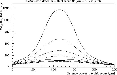
Figure:
Modulus of the weighting field for one strip,
for a ![]() thick GaAs microstrip
detector with
thick GaAs microstrip
detector with ![]() pitch and
pitch and ![]() metal. The different curves
refer to distances from
the strip plane differing by 25
metal. The different curves
refer to distances from
the strip plane differing by 25 ![]() .
.
A plot of the modulus of the weighting field for one strip is shown in fig. 2. The major contribution to the signal for that particular strip is due to holes or electrons moving in proximity of it. Due to the geometry, however most of the signal is due to holes.
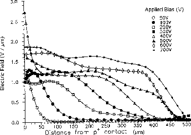
Figure 3:
Modulus of electric field profile measured by Berwick et al.
with a contact
probe on the cross section of a 500 ![]() -thick SIU-GaAs detector.
-thick SIU-GaAs detector.
The drift field was calculated by GARFIELD and then multiplied by the following function:
![]()
where x is the distance from the strip plane,
W = W(V) is the thickness of the active region, Wt is the thickness
of the transition region. A low overall constant field
of 100 V/cm was then added. The result is
an approximation to the field measured in ref. [7], (fig. 3).
It was assumed that ![]() with
with
![]() , as reported in [2].
, as reported in [2].
As an example, a zone of 550 ![]() in
width for a 200
in
width for a 200 ![]() thick detector was simulated. The
strip pitch was 50
thick detector was simulated. The
strip pitch was 50 ![]() and the metal width was 40
and the metal width was 40 ![]() .
Only the part comprising 5 central strips was used for further analysis
corresponding to a grid of
.
Only the part comprising 5 central strips was used for further analysis
corresponding to a grid of ![]() points.
Interpolation of the electric field was used between points.
points.
Interpolation of the electric field was used between points.