The present simulation chain can be a starting kernel for further improvements.
However, a more detailed simulation, including effects
of magnetic field and diffusion,
is possible if a definite shape of electric field is generally accepted.
Measurements made at UMIST [7] indicate that
the field is uniform
in the vicinity of the reverse biased contact, as shown in fig 3.
This a clear experimental result. Most calculations [4]
[5] result instead in a linearly decreasing electric field.
This arises naturally if a uniform doping concentration is assumed. Although
some of the defects are not ionized due to quasi-Fermi-level shifting by the
reverse bias
current, the main trend is a field decreasing monotonically to the
back contact. A constant electric field is quite difficult to explain.
A correlation between reverse current and
charge collection efficiency for alphas has been reported
as evidence supporting the calculations. This correlation has not been
found by us for m.i.p.s, as
we have several examples of detectors with a low reverse current density
(20 nA/mm2) and high charge collection efficiency (90 %)
over a large thickness
(500 ![]() ) (fig. 8).
) (fig. 8).
Another model [6] proposes a neutralization of deep levels by field-enhanced trapping of the electrons of the reverse current. In this model, too, a high current is required to obtain a high charge collection efficiency.
The nature of the reverse current is not yet clear. Thermionic emission would require a really low barrier height, while if a generation mechanism is assumed, saturation could normally be explained only if most of the current is generated in the first few micrometers below the reverse-biased contact. Otherwise the current density is expected to increase with the volume in which the electric field is high.
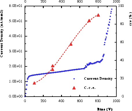
Figure:
Charge collection efficiency
for m.i.p.s and leakage current density at 20.0o C
for the SIU-GaAs pad detector G114-5.
The thickness is 500 ![]() , area is 7 mm2, with guard-ring.
, area is 7 mm2, with guard-ring.
Commercial SIU-GaAs usually contains a concentration of about
1016 cm-3
of EL2 defects. This defect
is believed to be due to an As substitutional
(AsGa) plus
an As interstitial (Asi) as second nearest neighbour [17].
The material is naturally compensated and shows a resistivity of ![]() cm
which is ideal in a substrate for electronic and optical circuits.
cm
which is ideal in a substrate for electronic and optical circuits.
The EL2 defect has been reported [9] to have a metastable state EL2* which has very little or no electrical and optical activity. It is therefore believed that the corresponding energy level is split and shifted into the conduction and valence bands. One proposed microscopic structure of EL2* is similar to EL2, but with the Asi atom as nearest neighbour. the transition is:
![]()
The EL2* can be generated via optical
absorption, involving different charge states [18].
The decay rate to the stable state has an activation energy of 0.3 eV so that
at room temperature the metastable state has a lifetime of about ![]() .
It is generally observed at fairly low temperatures, (about 77 K) and
in the presence of
a low electric field.
.
It is generally observed at fairly low temperatures, (about 77 K) and
in the presence of
a low electric field.
If the transition could happen at room temperature, under the effect of a high
electric field, for example,
the measurements of electric field shape in [7]
could be qualitatively explained in the following way:
as reverse bias is applied, deep donors start to become ionized;
some are
neutralized by trapping electrons from the leakage current, as in
[6]; this lowers their effective concentration, in such a way
that the electric field can extend for several micrometres. This process
continues until the field at the contact reaches a critical field, Ec,
of about 10 kV/cm, at a bias voltage between 20 and 50 V.
At this point the transition
EL2 ![]() EL2* starts to take place, so that the field
remains roughly constant, as deep levels are no loger active.
We should assume
that the transition is not complete, leaving some compensating EL2+.
The region where the field drops is shifted rigidly towards the back
contact as bias
is increased. In this transition
region the electric field is non-zero and most of the
EL2 defects are active. Thus the
reverse current can be efficiently generated there and
is constant to the extent that the transition region has a
constant thickness while
moving across. This is to be expected in a homogeneous material.
A sketch of the proposed model is shown in fig. 9.
EL2* starts to take place, so that the field
remains roughly constant, as deep levels are no loger active.
We should assume
that the transition is not complete, leaving some compensating EL2+.
The region where the field drops is shifted rigidly towards the back
contact as bias
is increased. In this transition
region the electric field is non-zero and most of the
EL2 defects are active. Thus the
reverse current can be efficiently generated there and
is constant to the extent that the transition region has a
constant thickness while
moving across. This is to be expected in a homogeneous material.
A sketch of the proposed model is shown in fig. 9.
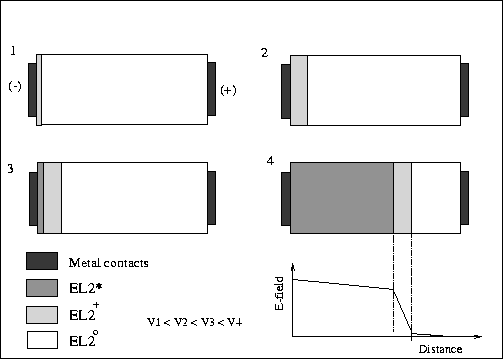
Figure 9:
Cross sections of a SIU-GaAs detector at different reverse bias voltages,
showing the regions
with a different predominant EL2 state.
From the point of view of charge transport, three regions of electric field
can therefore be distinguished:
one constant, one linearly decreasing and one with an
extremely low residual electric field.
This is quite similar to that shown in fig. 3.
In the third region transport is mainly due to charge relaxation,
with a typical time of
![]() , giving a slow signal component.
In the transition region the field is decreasing. Thus the electron
velocity initially increases then decreases and trapping can be enhanced.
The charge collection efficiency and
the medium-slow components of the signal depend on the shape of the field.
In the region where a constant field is present the charge transport is
good, as the concentration of active traps is lower. Little contribution to
trapping is expected from this zone.
, giving a slow signal component.
In the transition region the field is decreasing. Thus the electron
velocity initially increases then decreases and trapping can be enhanced.
The charge collection efficiency and
the medium-slow components of the signal depend on the shape of the field.
In the region where a constant field is present the charge transport is
good, as the concentration of active traps is lower. Little contribution to
trapping is expected from this zone.
The shape of electric field used in the simulation now has also a theoretical (although qualitative) explanation and is not based only on empirical data. While the validity of this model is not proved, it enables to explain consistently many features of SIU-GaAs detectors. C-V characteristics would not characterise this model, as the transition region where charge can move has the same features as in normal semiconductors. The saturation of reverse current can be explained in this model, assuming that the current is generated mainly in the transition region where the electric field is non negligible and the concentration of active levels is high.
A possible way to test the model is with OBIC measurements [2] using a focused light beam at a wavelength which is unable to separate directly an electron-hole pair. In this way only deep levels will be probed and the photocurrent at a distance from the front contact will be proportional to the number of active levels at that point and to the electric field. A region of constant width where the photocurrent is higher is expected to move across the detector as the reverse bias is increased. If the model is incorrect the region with high photoresponse will simply increase in width. We propose to carry out this measurement in the near future.