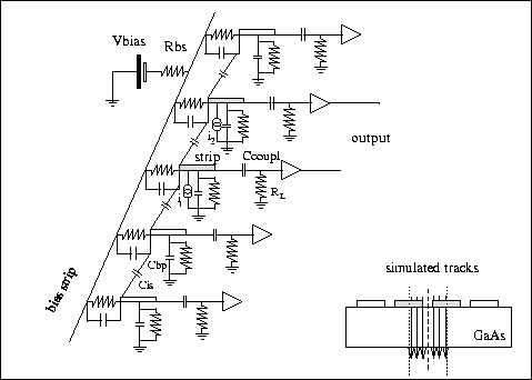
Figure 6:
Schematic of the circuit used in the SPICE simulation. Cis is the
inter-strip capacitance, Cbp is the capacitance to the backplane,
RL is the load resistance of the amplifier. The biasing structure is
represented by a parallel RC. Current sources from two neighbouring strips
are taken into account. An array of seven strips was simulated.
In order to calculate the signal reaching each preamplifier the front-end and
bias coupling network was simulated using SPICE. The parameters depend mainly
on the detector geometry. The main parameters are the inter-strip capacitance,
depending on pitch, aspect ratio and strip length, the strip to back contact
capacitance and the decoupling capacitance. The biasing structure, based on
punch-through was also included as a 10 G ![]() resistor with a 20 fF
capacitance in parallel. A schematic is shown in fig. 6. Resistors had to be
used to ensure a DC path to nodes.
resistor with a 20 fF
capacitance in parallel. A schematic is shown in fig. 6. Resistors had to be
used to ensure a DC path to nodes.
The signals from two neighbouring strips were included as two independent piece-wise linear current generators. The current values were calculated with the drift code described previously, simulating tracks impinging perpendicularly on the strips; the hit position was varied from the centre of the central strip to the centre of the neighbouring one on the right. It was assumed that all strips were read-out. In simulating the signal a symmetry relation was assumed, i.e. ij(t)|y=y0 = ij+1(t)|y=p-y0 where p is the pitch, and y0 is the distance of the track from the centre of the jth strip.
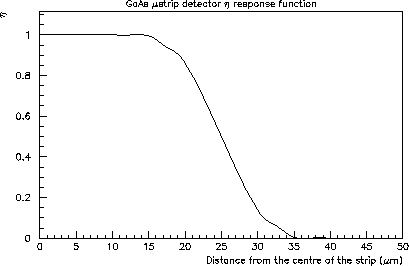
Figure 7:
Plot of the ![]() variable defined as:
variable defined as:
![]() ,
where x is the distance from the centre of the strip. The detector is
,
where x is the distance from the centre of the strip. The detector is
![]() thick, pitch is
thick, pitch is
![]() , metal width is
, metal width is ![]() .
.
The current signal at the preamplifier input was calculated and then
integrated to give the total charge detected by each channel. An ![]() function [16],
related directly to spatial resolution
could be calculated for the given configuration. An example is shown in fig. 7.
function [16],
related directly to spatial resolution
could be calculated for the given configuration. An example is shown in fig. 7.