The material used for the detectors was 200 ![]() m thick semi-insulating GaAs.
The detector fabrication was performed at the
University of Glasgow. The
detectors were designed with a circular pad contact and guard ring on top of the
substrate. The bottom
contact was a uniform contact that spread to the edge of the substrate.
Two geometries were used, one with a pad diameter of 2mm the other of 3mm; the
width of the guard was 200
m thick semi-insulating GaAs.
The detector fabrication was performed at the
University of Glasgow. The
detectors were designed with a circular pad contact and guard ring on top of the
substrate. The bottom
contact was a uniform contact that spread to the edge of the substrate.
Two geometries were used, one with a pad diameter of 2mm the other of 3mm; the
width of the guard was 200 ![]() m and
the pad guard
separation was 10
m and
the pad guard
separation was 10 ![]() m for both diameters. The pad and guard metallization
layers were identical and rectifying in nature. The
reverse contact had a different recipe but was also
rectifying,
however its saturation current was larger than the pad's due to its larger
surface area. In the following, the direction of the
detector bias is quoted with respect to that of the pad. Thus reverse bias means
that the
pad is at a negative potential with respect to the back contact.
m for both diameters. The pad and guard metallization
layers were identical and rectifying in nature. The
reverse contact had a different recipe but was also
rectifying,
however its saturation current was larger than the pad's due to its larger
surface area. In the following, the direction of the
detector bias is quoted with respect to that of the pad. Thus reverse bias means
that the
pad is at a negative potential with respect to the back contact.
The I-V curves obtained for the diodes in reverse and forward bias are shown in figure 2.
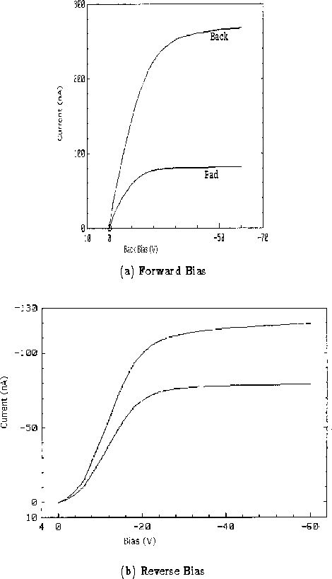
Figure 2: Current-Voltage characteristics, Temp=300K
The purpose of the guard ring was to ensure that the current through the pad remained constant once in saturation. This was observed for all the samples, with the current that flowed through the pad, in the bias range 60 to 200 volts, increasing by only a few percent. For a given bias the current densities of both pads were the same and equalled 25nA/mm2. The results showed that the saturation current density that flowed through the pad under forward bias was the same as that obtained in reverse bias.