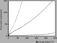
Figure 6 illustrates the significant change in the current characteristics after the
 cm
 proton fluence. The reverse current increased in the operating region of the detector and was
 85 nA/mm
 at a reverse bias of 150 V compared to only 4.6 nA/mm before irradiation. The forward current on the other hand was reduced after the fluence. The current characteristic was more resistive in nature and thus the resistivity of the material had increased. This implies that the product of the mobility and the free carrier concentration was reduced. A reduction in mobility is very likely as the increased number of defect centres will increase the concentration of scattering centres and thus reduce the mobility. The free carrier concentration will be reduced if deep levels are introduced which compensate the material and thus cause the Fermi level to approach mid-bandgap. The activation energy of the reverse current was measured at a bias of -10V and -100V to be
 eV if generation current was assumed. The change in activation energy was due to the presence of radiation induced deep levels.
|
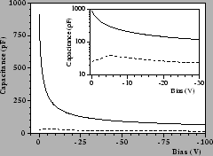
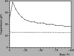
The capacitance-voltage relationship shows a dependence upon the frequency of the test signal used to make the measurement, illustrated in figure 7(a). The high frequency capacitance did not change with bias. This is characteristic of measurements made on high resistivity material where the capacitance measured with a high frequency test signal equals the geometrical capacitance of the device[5]. For this diode the measured capacitance at 100 kHz was 13 pF. The thickness of the VPE layer was not measured directly but a device of this capacitance implies that the diode is 110 m thick, which is in the expected range for the thickness of the VPE material.
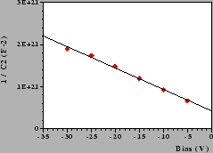
The capacitance voltage dependence before and after irradiation are compared in figure 7(b). The measured capacitance at a given bias fell and at -5 V was only 40 pF compared to 300 pF. As the measured capacitance depends upon the density of free carriers and the density of traps which have emission rates greater than the frequency of the A.C. test voltage, the reduction in the measured capacitance implies that the density of these carriers was reduced. Therefore a significant concentration of deep levels was created in the material due to the proton fluence. The effective trap concentration ( ) was deduced from the 1/C bias voltage dependence shown in figure 8, measured between -5 V and -30 V, to be only

 . The reduction in free carrier density measured as a fall in and as an increase in resistivity implies that either acceptor (electron) traps have been introduced and/or that the Fermi level has been lowered, resulting in a lower free carrier concentration. Lowering of the Fermi level will be caused by an increased concentration of deep levels that remove electrons from the conduction band, that is acceptor levels.
|
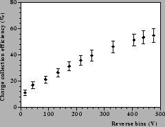
The charge collection efficiency of the irradiated device was investigated. Again results from high energy beta particles could not be obtained due to leakage current noise. The increase in reverse current also prevented the detection of 60 keV photons. Charge collection from front illumination by alpha particles was obtained and is illustrated in figure 9 as a function of bias. The cce fell from  100% before irradiation to
 % measured at 200V. The diode did not breakdown until higher voltages and a cce of 55% was measured at the highest possible voltage of 480 V.
 C.
 [Before and after irradiation measured with a test signal of 100 Hz. The key is: solid line - pre; dotted line - post.]